News
3D-Printed Optical Waveguides Lay Groundwork for Next Generation of Microelectronics

Using aerosol jet printing, Johns Hopkins APL researchers printed optical waveguides that successfully used light to detect physical phenomena. This successful demonstration marks a significant step toward the next generation of electronic and optical integrated microsystems for a variety of applications.
Credit: Bigstock
Microelectronics are ubiquitous in modern life; they are a common thread linking the smartphone in your pocket, the financial system processing your credit card, and the defense technologies deployed in austere environments. All of those disparate applications rely on advanced microelectronics to function, which means they all also share a common but urgent challenge: Today’s technology will not meet tomorrow’s demands.
Recognizing this fact, the White House released its National Strategy on Microelectronics Research in March. Among the strategy’s key points: a need for mission-specific functions that will drive diversification of microelectronics beyond current standard semiconductors, which in turn will be enabled and advanced by approaches such as heterogeneous integration and chiplets.
As part of a Defense Advanced Research Projects Agency (DARPA) seedling effort, researchers at the Johns Hopkins Applied Physics Laboratory (APL) in Laurel, Maryland, are exploring design and fabrication techniques to develop fully printed optical waveguides, which are physical structures that guide light and will be critical to the integration of photonic, as opposed to electronic, computing modalities in future bespoke microsystems.
Photonic microsystems — which use photons instead of electrons for computing functions — offer advantages in speed, sensing and complexity of computations and will soon become as ubiquitous as their electronic counterparts.
“As we move into the future, we are going to need to route both optical and electrical signals within microsystem packages to deliver the precise performance needed for a mission,” said Sarah Adams, the Alternative Computing Paradigms deputy program manager. “Our research was an ambitious effort to show how we could facilely fabricate fully customizable optical waveguides up, over and around complex geometries, just as we will need to do in the not-so-distant future.”
From Wires to Waveguides
The APL team recently laid the groundwork for integration of such complex, multimodal architectures by demonstrating printed optical waveguides on a simple electronic system. The researchers printed a waveguide up and over a packaged component and then verified its efficacy by transmitting light through the waveguide into a sensor. This demonstration leveraged an additive manufacturing technique called aerosol jet printing, a technology that allows the team to work with multiple materials and in complex geometrical constraints.
“Think of it as having a really tiny spray paint can. Just like when you spray-paint something, you don’t touch the surface like you would with a paintbrush,” said Adams. “When we use this technique, we’re printing from about five millimeters from the surface; this gives us design freedom not accessible by conventional fabrication techniques.”
Conventional electronics and photonics fabrication techniques rely on subtractive processes: covering a substrate in layers of a material and etching away the areas where the material isn’t needed for the design.
“With conventional fabrication, you always need a primary design that you’re making copies of,” Adams said. “Just as you get design freedom when you go from milling to 3D printing, you get design freedom when you go from traditional processes to additively manufactured electronics.”
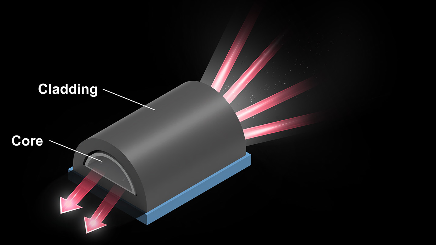
A graphic illustration of the 3D-printed waveguide developed by APL researchers. These structures guide data-transmitting light and will be critical to the integration of photonic computing modalities in future bespoke microsystems.
Credit: Johns Hopkins APL/Claire DeSmit and Karim Whalen
The Power of Design Freedom
Design freedom, in turn, allows for the creation of custom microsystems for mission-specific needs. Not only is the printing technique surface-agnostic, it also allows for the printing of fine features into arbitrarily complex designs.
Case in point: The printing technology used by Adams and her team can produce features from 10 micrometers up to a few millimeters in size, spanning three orders of magnitude as needed to accommodate design changes on the fly. Moreover, the process can accommodate multiple materials, allowing the team to form a core and cladding — necessary features for containing light within a waveguide. In all, the team developed a library of about a dozen optical inks to form waveguides that can be carefully tailored to the needed application.
As a demonstration of the robustness of this print technology and materials, a series of optical waveguides were printed from two APL-developed materials. These waveguides measured roughly 500 micrometers in width and connected an LED light source to a photodetector. Together, the LED, waveguide and photodetector were used as a stress sensor; as the substrate was strained, the light-capturing properties of the waveguide changed, affecting how much light reached the sensor.
The printed waveguides were tested in APL’s Environmental Test Facility, including vibration testing at up to 20 times the force of gravity and thermal cycling from negative 15 degrees to positive 60 degrees Celsius. Throughout this rigorous testing, the waveguides remained robust; the technology developed by APL was shown to detect only the stimulus of interest and not the environmental conditions. This demonstration showcased that this advanced fabrication technique may be useful in a broad range of environments.
Pushing Printing Further
The team has plans to continue optimizing system design to further leverage sensor properties while exploring ideal materials for containing and refracting light within the waveguides. The team is also interested in pushing the resolution envelope on aerosol jet printing toward even finer feature sizes for applications in photonic integrated circuits.
“As it becomes more challenging to drive processing power by increasing the density of transistors, researchers will need to deploy new computing modalities in a modular, customizable fashion,” said Joan Hoffmann, program manager for Alternative Computing Paradigms at APL.
“Additive techniques like aerosol jet printing are key enablers for flexible microsystem fabrication — using exactly the right technologies and components to meet stringent demands,” she said. “As we move into an era of hybrid computing, printed waveguides will enable new solutions.”
DISTRIBUTION STATEMENT A. Approved for public release. Distribution is unlimited. The views, opinions and/or findings expressed are those of the author(s) and should not be interpreted as representing the official views or policies of the Department of Defense or the U.S. Government.
Capabilities
Design, Engineering, and Fabrication
At APL, our culture of taking bold risks, brought to life through inventive prototyping and informed by deep technical expertise, is the basis for our efforts to not merely anticipate the future, but create it. Learn more about our design, engineering, and fabrication capabilities.